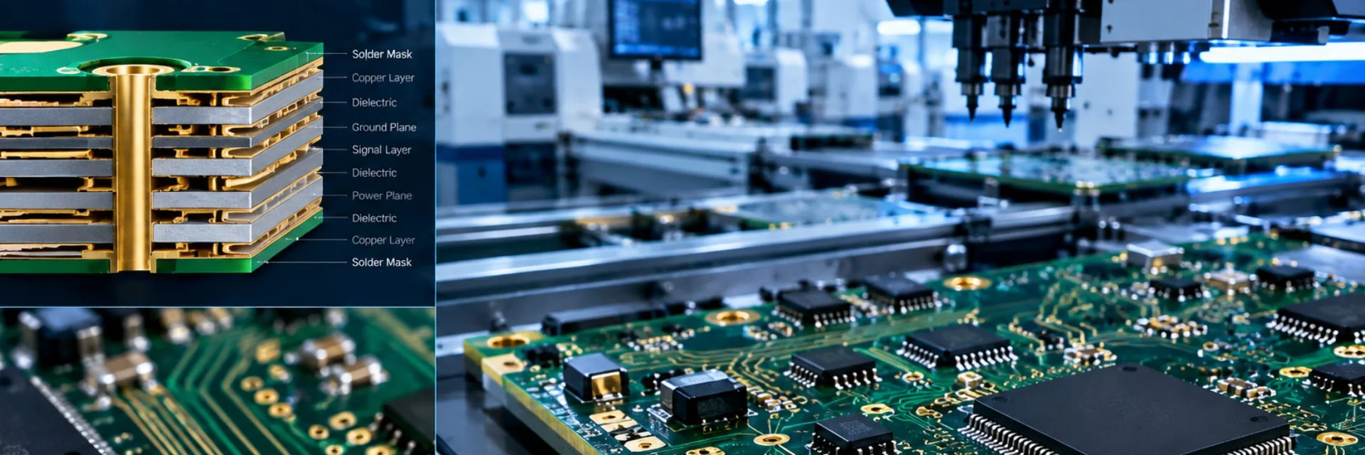
Precision PCB Fabrication & Turnkey PCBA Assembly
Industrial-grade bare boards and surface-mount assembly engineered for mission-critical hardware. From 24-hour quick-turn prototypes to scalable high-density multi-layer production runs.
Real-Time PCB Specification Calculator
Customize board layers, substrate materials, thickness, surface finishes, and batch quantities with live turnaround calculations.
PCB Manufacturing Technical Capability Matrix
Certified limits for standard commercial fabrication versus advanced prototype production according to IPC-6012 and IPC-A-600 standards.
| Parameter Category | Standard Capability | Advanced / Prototype | Tolerance / Standard |
|---|---|---|---|
| Layer Count | 1 – 16 Layers | Up to 32 Layers | IPC Class 2 / 3 |
| Base Materials | FR4 (Tg140/Tg170), Aluminum Core | Rogers 4350B, Polyimide Flex, Megtron 6 | IPC-4101D |
| Board Thickness | 0.4mm – 3.2mm | 0.2mm – 6.0mm | ±10% (±0.1mm) |
| Maximum Dimensions | 500mm × 600mm | 600mm × 1200mm (Heavy Panel) | ±0.2mm |
| Min Track / Spacing | 4mil / 4mil (0.10mm) | 3mil / 3mil (0.075mm) | ±20% etching limit |
| Min Mechanical Hole | 0.20mm (8mil) | 0.15mm (6mil) | PTH ±0.05mm / NPTH ±0.025mm |
| Laser Micro-Via | 0.10mm (4mil) | 0.075mm (3mil) | HDI Blind / Buried Vias |
| Aspect Ratio (Thickness:Hole) | 8 : 1 | 12 : 1 | Uniform copper plating |
| Finished Copper Weight | 1oz – 3oz | 4oz – 6oz (Heavy Copper) | IPC-6012 Class 3 |
| Solder Mask Bridge | 4mil (0.10mm) | 3mil (0.075mm) | LPI Solder Mask |
| Impedance Control | ±10% (Differential / Single) | ±5% Precision Control | Polar SI9000 & TDR Coupon |
| Surface Finishes | Lead-Free HASL, ENIG, OSP | Immersion Silver, Hard Gold, ENEPIG | RoHS / REACH Compliant |
Fabrication Geometry & Cross-Section Reference Standards

Trace Width & Spacing
3mil minimum conductor width with strict impedance-controlled cross-sections.
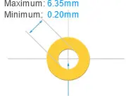
PTH & Annular Ring
Hole wall copper plating >20µm with minimum annular ring for tear resistance.
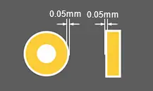
Mask Dam & Clearance
3mil minimum solder dam between fine-pitch QFP/BGA pads preventing solder bridges.
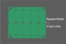
V-Score & Mouse Bites
Optimized breakout tabs and 30° V-scoring angles designed for clean automated de-paneling.
Turnkey PCBA Assembly Standards & Line Specifications
Advanced high-speed automated assembly lines delivering complete board manufacturing, precision component placement, and comprehensive structural inspection.
Precision SMT Placement
Yamaha & Panasonic high-speed pick-and-place lines supporting passives down to 01005 (0.4×0.2mm) and ultra-fine pitch BGA down to 0.35mm ball pitch with ±0.03mm accuracy.
3D SPI & AOI Inspection
Inline 3D Solder Paste Inspection (SPI) checks solder height and volume before component placement. 3D Automated Optical Inspection (AOI) catches coplanarity and polarity flaws.
Transmission 3D X-Ray
Dedicated high-magnification transmission X-ray diagnostic stations inspecting solder voids beneath BGA balls, QFN thermal pads, and hidden lead-less packages.
Conformal Coating & FCT
Automated selective robotic conformal coating (silicone/acrylic/polyurethane), firmware flashing, and custom bed-of-nails Functional Circuit Testing (FCT).
Need Full Turnkey Box-Build or Complete PCBA?
Combine component procurement, bare board fabrication, SMT assembly, and FCT functional testing under a single contract with unified warranty coverage.